
- 非IC关键词
深圳市中立信电子科技有限公司

- 卖家积分:
 营业执照:已审核经营模式:贸易/代理/分销所在地区:广东 深圳企业网站:
http://www.zlxele.com
收藏本公司 人气:716935
企业档案
- 相关证件:

- 会员类型:
- 会员年限:16年
- 叶先生

- 电话:0755-23956688
- 手机:13410226883
- 王先生
- 电话:0755-23956688
- 阿库IM:
- 地址:深圳市福田区彩田路彩虹新都大厦彩荟阁7A室
- 传真:0755-23956688
- E-mail:Lee@zlxele.com
产品分类
- 超高频/高频三极管(18)
- 复合(达林顿)三极管(2)
- 其他三极管(55)
- 单向可控硅(晶闸管)(2)
- 双向可控硅(晶闸管)(16)
- 可控硅(晶闸管)模块(10)
- 其他电位器(9)
- 模块电源/电源模块(1)
- 其他微调/预调电位器(1)
- 背板连接器(1)
- 气体放电管(1)
- 其他继电器(1)
- 红外线发射管(1)
- 光电光耦合器(光耦)(11)
- LED器件(54)
- 其它LED相关产品(服务)(1)
- 整体式PLC(1)
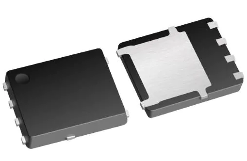


NTMFS4C022NT1G MOSFET ON
NTMFS4C022NT1G
ON(安森美)
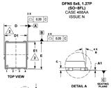
SO-8
无铅环保型
贴片式
卷带编带包装
1500/5000
Reel
30 V
20 V
相关产品


产品信息
NTMFS4C022NT1G
Power MOSFET 30 V, 2.1 m, 136 A, Single N−Channel, SO−8FL
Features NTMFS4C022NT1G
• Small Footprint (5x6 mm) for Compact Design
• Low RDS(on) to Minimize Conduction Losses
• Low QG and Capacitance to Minimize Driver Losses
• These Devices are Pb−Free, Halogen Free/BFR Free and are RoHS Compliant
Stresses exceeding those listed in the Maximum Ratings table may damage the
device. If any of these limits are exceeded, device functionality should not be
assumed, damage may occur and reliability may be affected.
NTMFS4C022NT1G THERMAL RESISTANCE MAXIMUM RATINGS (Note 1)
Parameter Symbol Value Unit
Junction−to−Case − Steady State (Note 2) RJC 1.95 °C/W
Junction−to−Ambient − Steady State (Note 2) RJA 40
1. The entire application environment impacts the thermal resistance values shown,
they are not constants and are only valid for the particular conditions noted.
2. Surface−mounted on FR4 board using a 650 mm2, 2 oz. Cu pad.
3. Maximum current for pulses as long as 1 second is higher but is dependent
on pulse duration and duty cycle.
MAXIMUM RATINGS (TJ = 25°C unless otherwise noted) NTMFS4C022NT1G
Parameter Symbol Value Unit Drain−to−Source Voltage VDSS 30 V Gate−to−Source Voltage VGS 20 V Continuous Drain Current RJC (Notes 1, 3) Steady State TC = 25°C ID 136 A Power Dissipation RJC (Notes 1, 3) TC = 25°C PD 64 W Continuous Drain Current RJA (Notes 1, 2, 3) Steady State TA = 25°C ID 30 A Power Dissipation RJA (Notes 1, 2, 3) TA = 25°C PD 3.1 W Pulsed Drain Current TA = 25°C, tp = 10 s IDM 352 A Operating Junction and Storage Temperature TJ, Tstg −55 to 150 °C Source Current (Body Diode) IS 53 A Single Pulse Drain−to−Source Avalanche Energy (IL(pk) = 11 A) EAS 549 mJ Lead Temperature for Soldering Purposes (1/8″ from case for 10 s) TL 260 °C Stre

