- 非IC关键词
深圳市中立信电子科技有限公司

- 卖家积分:
 营业执照:已审核经营模式:贸易/代理/分销所在地区:广东 深圳企业网站:
http://www.zlxele.com
收藏本公司 人气:697143
企业档案
- 相关证件:

- 会员类型:
- 会员年限:16年
- 叶先生

- 电话:0755-23956688
- 手机:13410226883
- 王先生
- 电话:0755-23956688
- 阿库IM:
- 地址:深圳市福田区彩田路彩虹新都大厦彩荟阁7A室
- 传真:0755-23956688
- E-mail:Lee@zlxele.com
产品分类
- 超高频/高频三极管(18)
- 复合(达林顿)三极管(2)
- 其他三极管(55)
- 单向可控硅(晶闸管)(2)
- 双向可控硅(晶闸管)(16)
- 可控硅(晶闸管)模块(10)
- 其他电位器(9)
- 模块电源/电源模块(1)
- 其他微调/预调电位器(1)
- 背板连接器(1)
- 气体放电管(1)
- 其他继电器(1)
- 红外线发射管(1)
- 光电光耦合器(光耦)(11)
- LED器件(54)
- 其它LED相关产品(服务)(1)
- 整体式PLC(1)


ADG3123BRUZ 转换 - 电压电平
: Translation - Voltage Levels
: 80 ns
: 5.5 V
: 2.3 V
: - 40 C
: + 85 C
相关产品

产品信息
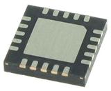
ADG3123BRUZ
转换 - 电压电平 8CH CMOS Logic to High-Voltage
8-Channel CMOS Logic to High Voltage Level Translator
FEATURES ADG3123BRUZ
2.3 V to 5.5 V input voltage range
Output voltage levels (VDDA and VDDB to VSS ≤ 35 V)
Low output voltage levels: down to −24.2 V
High output voltage levels: up to +35 V
Rise/fall time: 12 ns/19.5 ns typical
Propagation delay: 80 ns typical
Operating frequency: 100 kHz typical
Ultralow quiescent current: 65 μA typical
20-lead, Pb-free, TSSOP package
APPLICATIONS ADG3123BRUZ
Low voltage to high voltage translation
TFT-LCD panels
Piezoelectric motor drivers
GENERAL DESCRIPTION ADG3123BRUZ
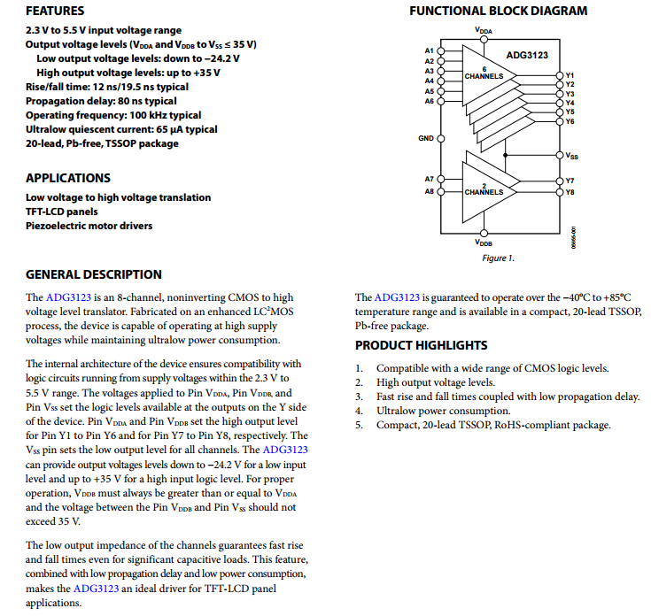
The ADG3123 is an 8-channel, noninverting CMOS to high voltage level translator. Fabricated on an enhanced LC2 MOS process, the device is capable of operating at high supply voltages while maintaining ultralow power consumption.
The internal architecture of the device ensures compatibility with logic circuits running from supply voltages within the 2.3 V to 5.5 V range. The voltages applied to Pin VDDA, Pin VDDB, and Pin VSS set the logic levels available at the outputs on the Y side of the device. Pin VDDA and Pin VDDB set the high output level for Pin Y1 to Pin Y6 and for Pin Y7 to Pin Y8, respectively. The VSS pin sets the low output level for all channels. The ADG3123 can provide output voltages levels down to −24.2 V for a low input level and up to +35 V for a high input logic level. For proper operation, VDDB must always be greater than or equal to VDDA and the voltage between the Pin VDDB and Pin VSS should not exceed 35 V.